


Ads by Google


| Surface processing type | HASL/ plating gold /immersion gold/ Ni/Au plating gold finger/OSP processing/immersion Tin /immersion siler |
| Layers | single-sided,double-sided,multilayer pcb board |
| Min trace width | 6mil |
| Min space width | 3mil |
| Min trace to pad/pad to pad space | 6mil |
| Min drill diameter | 8mil |
| Min via pad | 24mil |
| Max board size | Single and double sides:550mmX1100mm;multilayer:550mmX640mm |
| Min solder mask dam | 6mil |
| Min solder mask clearance | 1.5mil |
| Min solder mask thickness | 10um |
| Solder mask type | Green/yellow/black/red/white/blue or transparent photosensitive solder mask and peel off blue glue. |
| Min silk legend width | 6mil |
| Min silk legend height | 25mil |
| Silk legend color | White/ yellow /black |
| Data file format | GERBER file and corresponding drilling file,PROTEL series,PADS2000,POWERPCB series,ODB++ |
| Electricity performance testing | 100% electrical performance testing,high pressure testing |
| Power Various types base material to PCB processing | High TG board, high frequency board(ROGERS,TEFLON) halogen-free board (FR-4,CEM-1,CEM-3) |
| Other testing request | Impendence testing, Hole resistance testing, gold slice up, Solder ability. |
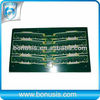
laptop Electronic Multilayer PCB Board with pcb design