


Ads by Google

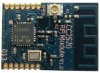

The VT-CC2520-Z1 Wireless Module use TI's second generation ZigBee® / IEEE 802.15.4 RF transceiver for the 2.4 GHz unlicensed ISM band. In a typical system, This module can be used together with a microcontroller.
Featuresl ZigBee/IEEE 802.15.4 RF transceiver for the 2.4 GHZ unlicensed ISM band
l Programmable output power up to +5 dBm,Excellent receiver sensitivity (-98 dBm)
l Provides extensive hardware support for frame handling, data buffering, burst transmissions, data encryption, data authentication, clear channel assessment, link quality indication and frame timing information. These features reduce the load on the host controller
l 6 configurable IO pins
l 128 bit AES
l CC2420 compatibility mode
l Wide supply range: 1.8 V – 3.8 V
l Suitable for systems targeting compliance with worldwide radio frequency regulations: ETSI EN 300 328 and EN 300 440 class 2 (Europe), FCC CFR47 Part 15 (US) and ARIB STD-T66 (Japan)
l Small Size 23.0*16.0*2.0mm
Applicationl 2.4GHz IEEE 802.15.4/ZigBee systems
l Home and building automation
l Set-top boxes and remote controls
l Industrial monitoring and control
l Automatic Meter Reading
l Consumer electronics
l Low-power wireless sensor networks
ParameterPARAMETER | TYP | REMARK | |
Frequency range | 2394-2507MHz | ||
Frequency error | +/-10ppm | ||
Modulation | O-QPSK | ||
Data rate | 250Kbps | ||
Output power | -20 ~ +5dBm | Programmable | |
Transmit current | ≤38mA | ||
Receiver sensitivity | -98dBm | ||
Receive current | ≤25mA | ||
Sleep current | LPM1 | ≤250uA | XOSC off, digital regulator on. State retention. |
LPM2 | ≤120nA | XOSC off, digital regulator off. No state retention. | |
Supply voltage | 1.8-3.8V | ||
Operating temperature | -20°C ~75°C | ||
Dimension | 23.0*16.0*2.0mm | ||
PIN | Type | Description |
VCC | Power | 1.8 V to 3.8 V analog power supply connections |
GND | Ground | |
GPIO0 | IO | General purpose digital I/O |
GPIO1 | IO | General purpose digital I/O |
GPIO2 | IO | General purpose digital I/O |
GPIO3 | IO | General purpose digital I/O |
GPIO4 | IO | General purpose digital I/O |
GPIO5 | IO | General purpose digital I/O |
CSN | I | SPI interface: Chip Select, active low |
SI | I | SPI interface: Serial In |
SO | O | SPI interface: Serial Out |
SCLK | I | SPI interface: Serial Clock. Maximum 8 MHz |
VREG | I | When high, digital voltage regulator is active |
RESET | I | External reset pin, active low |
IPEX | Antenna | When use optional antenna outside, place 0 Ohm at R2 and no longer use R1. The antenna impedance is 50 Ohm. |