

Ads by Google


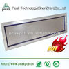
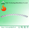
Welcom To peakpcb: Professional PCB&PCBA Manufacturer: shenzhen manufacturer double sided LED Strip FPCB
1 About us Peakpcb technology
Peak technology (shenzhen) corporation limited is a professional PCB manufacturer, with the strength of 1 - 12 layers of PCB and 1-6 layers of FPC production. Our business are ranging from PCB & PCBA design and copy, to PCB manufacture. Our products are widely used in communication apparatus, automobile electronics, computers, medical devices, light systems, outdoor systems, network devices and consumer electronics class fields. Welcome to send us your inquiry.
We have 3 years gold supplier experiences with alibaba.
We offer quick turn pcbs production for our customers:
1-2 layer in 48 hours, 4 layer in 72 hours, 6 layer in 96 hours
2 Quotation required:
1) Gerber file / PCB file 2) Clear pictures of pcb/ fpc/ pcba or pcba sample 3) The PCB specification: base material, board thickness, copper thickness, surface finishing, gold immersion thickness, and any other special requirements.4) Test method for PCB/PCBA
3 Delivery Time for Hi-frequency PCB
1) Sample within 6 days for high frequency board
2) Normal pcb within 4 days for sample
3) Quick turn PCB within 48 hours
4 Maximum Process PCB Capability of Our Company
Item | Manufacture Capability | |
Material | FR-4 / Lead free Materials (RoHS Compliant) /CEM-3, Aluminium, Metal based | |
Layer No. | 1-12 | |
Finished Board thickness | 0.2 mm-3.8mm’(8 mil-150 mil) | |
Board Thickness Tolerance | ±10% | |
Cooper thickness | 0.5 OZ-2OZ | |
Copper Plating Hole | 18-40 um | |
Impedance Control | ±10% | |
Warp&Twist | 0.70% | |
Peelable | 0.012"(0.3mm)-0.02’(0.5mm) | |
Images | ||
Min Trace Width (a) | 0.1mm (4 mil) | |
Min Space Width (b) | 0.1mm (4 mil) | |
Min Annular Ring | 0.1mm (4 mil) | |
SMD Pitch (a) | 0.2 mm(8 mil) | |
BGA Pitch (b) | 0.2 mm (8 mil) | |
Solder Mask | ||
Min Solder Mask Dam (a) | 0.0635 mm (2.5mil) |
|
Soldermask Clearance (b) | 0.1mm (4 mil) | |
Min SMT Pad spacing (c) | 0.1mm (4 mil) | |
Solder Mask Thickness | 0.0007"(0.018mm) | |
Holes | ||
Min Hole size (CNC) | 0.2 mm (8 mil) | |
Min Punch Hole Size | 0.9 mm (35 mil) | |
Hole Size Tol (+/-) | PTH:±0.075mm;NPTH: ±0.05mm | |
Hole Position Tol | ±0.075mm | |
Plating | ||
HASL | 2.5um | |
Lead free HASL | 2.5um | |
Immersion Gold | Nickel 3-7um Au:1-5u'' | |
OSP | 0.2-0.5um | |
Outline | ||
Panel Outline Tol (+/-) | CNC: ±0.125mm, Punching: ±0.15mm | |
Beveling | 30°45° | |
Gold Finger angle | 15° 30° 45° 60° | |
Certificate | ROHS, ISO9001:2008, SGS, UL certificate | |
5 Factory workshops and the pcb equipments
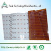
Other types of pcb product display
6 PCB Product certification
led pcb | pcb and pcba manufacturer of peakpcb