


Ads by Google


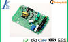
multilayer printed circuit board
*Base material: FR-4
*Copper thickness: 0.5-2.0 oz
*Thickness: 0.2-3.0mm
*Solder mask: green, black, red ,yellow, white
*Min. line width: 0.2mm
*Min. line space: 0.2mm
*Min. hole diameter: 0.25mm
*Max board size : 600 x 1200mm
*Surface treatment: spray tin, Gold-plating.immersed gold,OSP
*lead time: seven days
Layer count | 1-20 |
Mine line width/space | 4mil/4mil(100um/100um) |
Thickness of inner copper | 1/3oz,1/2oz,1oz,2oz,3oz |
Thickness of finished panel | 0.2-4.0mm |
Tolerance of finished panel thickness | Thickness< 0.5mm ±0.05 Thickness≥0.6-1.0mm ±10% Thickness>1.2mm ±0.127 |
Min diameter of finished hole | 0.20mm |
Min drilling diameter | 0.20mm |
Thickness of solder mask | Line end 0.4-1.2mil Line comer ≥0.2mil |
Hardness of solder mask | 6H |
Min solder mask dam | 4.0mil(100um) |
Max solder mask plug hole diameter | 0.6mm |
V-cut angle | 25°,30°,45°,60° |
Range of bevel ange | 25°-60° |
Warp and twist | ≤0.5% |
Surface treatment | HAL/HAL lead free,gold finger,OSP,silver,gold |
Type of ccl material | FR-4,AL,CEM-1,CEM-3,TG 180 |
SERVICE:
1) procurement agent electronic components,share with the best quanlity best price's electronic components in Chinese Market.2) Plug-in electronic components,Patch processing.Pls save trouble,and hand in them for us,We always try our best to do it.3) Testing PCBA.Assurance of all your product are work well in hand.
ENTERED PICTURES
WELCOME TO VISIT OUR HOME
Multilayer Printed Circuit Board service,PCB copy service